Popular Keywords
News
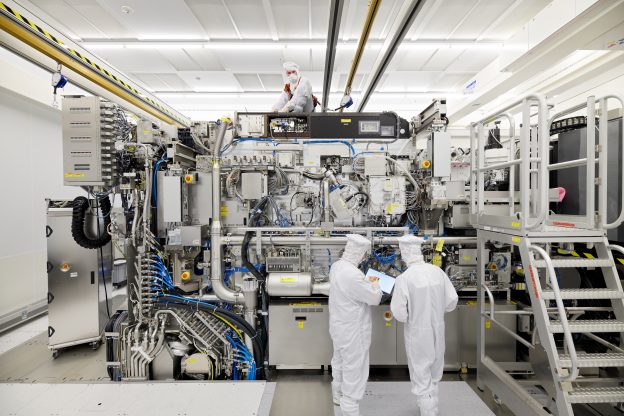
[News] Price for ASML’s Hyper-NA EUV Rumored to Double, Causing TSMC, Samsung and Intel to Hesitate
Semiconductor equipment giant ASML plans to launch Hyper-NA Extreme Ultraviolet (EUV) machines by 2030, signaling the advent of the Angstrom era for semiconductor processes below 1 nanometer. However, according to a report from The Chosun Daily, the high cost of this equipment may cause TSMC, Samsung, and Intel to hesitate.
Reportedly, it’s said that ASML introduced a higher numerical aperture (high-NA) EUV machine last year, which outperforms existing EUV technology. Now, ASML is rumored to release the Hyper-NA EUV for sub-1nm processes by 2030. This development brings up significant strategic considerations for TSMC, Samsung, and Intel due to the substantial expense involved in acquiring such advanced equipment.
According to the report, currently, each EUV machine costs approximately USD 181 million. The new generation high-NA EUV machines cost from USD 290 million to USD 362 million per unit, while the expected cost for Hyper-NA EUV could exceed USD 724 million, namely, about twice the price of the previous generation.
The same report further points out that TSMC plans to maximize the capabilities of its existing EUV equipment and utilize them through multi-patterning techniques. Simultaneously, the company is evaluating the scale at which additional equipment may be introduced.
A source cited in the report mentioned that though TSMC adopted EUV technology after Samsung, it has managed to mitigate the investment burden of adopting new equipment by upgrading existing tools and employing multi-patterning techniques effectively.
The same source also indicated that TSMC is particularly interested in multi-patterning techniques. By leveraging its extensive expertise and existing EUV infrastructure, TSMC has developed multi-patterning processes, aiming to delay the adoption of high-NA and Hyper-NA EUV as much as possible.
TSMC has openly expressed concerns about the high cost of the new generation high-NA EUV machines. TSMC’s Senior Vice President of Business Development and Co-Chief Operating Officer, Dr. Kevin Zhang, has indicated that the development of 1.6 nanometer processes may not necessarily require high-NA technology.
Zhang further mentioned that the decision to adopt the new ASML technology would depend on where it offers the most economic benefits and the technical balance they can achieve. He declined to disclose when TSMC might purchase High-NA EUV from ASML.
As per the same report, Samsung is also considering the adoption of high-NA equipment but is adjusting its long-term roadmap with the emergence of Hyper-NA. According to another source cited by the report, it claimed that choosing high-NA now may not be the best option for long-term plans that involve processes below 1 nanometer.
The source continued that given the emergence of Hyper-NA, one approach might be to maximize the use of existing EUV and skip high-NA, transitioning directly to Hyper-NA. However, this is under the premise that Hyper-NA equipment has reached a certain level of reliability.
Intel was the first foundry to adopt high-NA EUV technology. Last year, its foundry business suffered a USD 7 billion loss, and in the first quarter of this year, it faced a record operational loss. One of the reasons for these financial challenges may be contributed to the cost burden of being an early adopter of the next-generation EUV equipment.
ASML has stated that high-NA EUV will enable Intel to produce chips with process nodes from 2 nanometers down to 14 angstroms (1.4 nanometers) and from 10 angstroms (1 nanometer) down to 7 angstroms (0.7 nanometers). ASML also mentioned that Hyper-NA will be essential for future angstrom-scale processes, as it can reduce the risks associated with multi-patterning processes, the report noted.
Read more
- [News] How Costly is the High-NA EUV? TSMC Reportedly Shocked, Considering Not Using the Equipment in its A16 Node
- [News] EUV as a Strategic Asset in the Most Advanced Processes: Progress in Intel/TSMC/Samsung’s Adoptions
(Photo credit: ASML)
Please note that this article cites information from The Chosun Daily.


