Popular Keywords
News
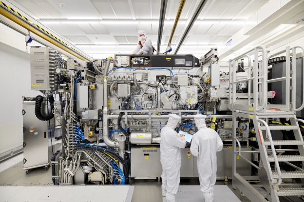
[News] Samsung’s 2nm Node Will Reportedly Feature 30% More EUV Layers
As the industry is entering the Angstrom era with semiconductor giants eagerly applying EUV machines to the advanced nodes, more details about Samsung’s 2nm have surfaced. According to the latest report by TheElec, Samsung’s 2nm process will feature 30% more extreme ultraviolet (EUV) layers than the 3nm node.
The report notes that Samsung’s 3nm node has 20 EUV mask layers, while the layers of the 2nm node will be increased to late-20. As the cost of manufacturing rises with the number of EUV mask layers, whether the wafer average selling price of Samsung’s 2nm will significantly increase attracts attention.
According to the report, the South Korean semiconductor giant first implemented EUV technology in its logic process nodes with 7nm in 2018. Since then, Samsung has increased the number of EUV layers or process steps with each subsequent node, moving from 5nm to 3nm. The report also states that Samsung’s 1.4nm process, set to begin production in 2027, is expected to feature over 30 EUV layers.
Meanwhile, Samsung is also using EUV in its DRAM production. For its Gen 6 10nm DRAM, Samsung has implemented up to 7 EUV layers, compared to 5 layers used by SK Hynix, TheElec states.
In comparison, according to an earlier report by AnandTech, TSMC’s standard N3 node includes up to 25 EUV layers. TSMC employs EUV double-patterning on some of these layers to achieve greater logic and SRAM transistor density compared to its N5 node.
It is also worth noting that as EUV layers increase with each node, foundries are vying to secure more EUV machines from ASML. The Dutch lithography equipment giant is said to ship over 70 EUV machines to TSMC in 2024 and 2025 in response to the strong demand of 2nm and 3nm, according to a report by MoneyDJ.
Read more
- [News] Samsung Officially Secures Its First 2nm Order, Making AI Chips for Preferred Networks
- [News] Intel Secures First Batch of High-NA EUV Equipment from ASML, Ahead of Samsung and SK Hynix
(Photo credit: ASML)


