TrendForce News operates independently from our research team, curating key semiconductor and tech updates to support timely, informed decisions.
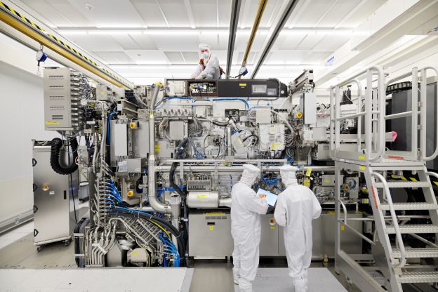
As semiconductor giants, starting with Intel and TSMC, have been bringing in ASML’s High-NA EUV (high-numerical aperture extreme ultraviolet) equipment to accelerate the development in advanced nodes, the elite group has now reportedly been added two new members: Samsung and SK hynix.
According to the reports by Korean media outlet Sedaily and ZDNet, Samsung Electronics’ semiconductor (DS) division is said to bring in High-NA EUV equipment as early as the end of 2024. SK hynix’s High-NA equipment, which is expected to be applied to the mass production of advanced DRAM, will reportedly be introduced in 2026.
Samsung to Introduce First High-NA EUV Machine as soon as Year-End, Eyeing Full Commercialization by 2027
Sedaily, citing industry sources on August 13th, notes that Samsung is expected to begin bringing in its first High-NA EUV equipment, ASML’s EXE:5000, between the end of this year and the first quarter of next year. It is worth noting that Samsung’s first High-NA EUV equipment is likely to be used for foundry operations, the report reveals.
Among the semiconductor heavyweights which have been advancing in the foundry business, Intel is the first to order new High-NA EUV machines from ASML. In May, Intel was said to have secured its first batch of the new High-NA EUV lithography equipment from ASML, which the company will allegedly use on its 18A (1.8nm) and 14A (1.4nm) nodes.
TSMC, on the other hand, is more concerned on the new machine’s expensiveness, as it might be priced at as much as EUR 350 million (roughly USD 380 million) per unit, according to a previous report by Bloomberg. However, the report, citing ASML’s spokesperson, confirmed that the Dutch chip equipment giant will ship High-NA EUV equipment to TSMC by the end of this year.
Now, following its two major rivals in the foundry sector, Samsung, by introducing High-NA EUV equipment as soon as year-end, aims to boost its competitive edge in the advanced nodes.
As the installation process is quite time-consuming, Samsung aims for the full commercialization of High-NA by 2027, supported by its efforts to build the related ecosystem, the report says.
According to the report, Samsung is working with electronic design automation (EDA) companies to design new types of masks, including curved (curvilinear) circuits for High-NA EUV that improve the sharpness of the printed circuits on wafers. This collaboration includes companies like Synopsys, a global leader in semiconductor EDA tools.
SK hynix’s High-NA EUV Reportedly to be Applied to 0a DRAM Production
According to the report by Sedaily, ASML has produced eight EXE:5000 High-NA EUV units currently, as Intel has the lion’s share by securing multiple units. Samsung is said to be the last customer to place the order for ASML’s first batch of units.
On the other hand, SK hynix, Samsung’s major rival in the memory sector, is reported to bring in ASML’s next generation of High-NA EUV machine, the EXE:5200, in 2026, ZDNet suggests.
Citing industry sources on August 16th, ZDNet notes that the HBM giant has been expanding the personnel dedicated to High-NA EUV development within the company.
Although specific plans, such as the fab where the equipment will be installed or the direction of additional investment, have not been disclosed, it is expected that the technology could be applied to mass production in 0a (single-digit nanometer) DRAM as early as possible, the report indicates.
Read more
(Photo credit: ASML)