News

According to a report from TechNews, citing a report from Nikkei, TSMC is set to receive ASML’s most advanced High NA EUV lithography machines before the end of the year.
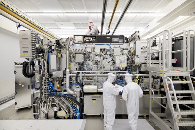
The machine, known as high numerical aperture extreme ultraviolet (High NA EUV) lithography equipment, costs over USD 350 million each and allows semiconductor manufacturers to produce wafers with smaller transistor line widths, according to Nikkei.
The report indicated that TSMC is likely to use the machines for its angstrom 10 (A10) technology, expected to enter mass production sometime after 2030. The A10 technology is about two generations ahead of the 2-nm chips that TSMC plans to mass produce by the end of 2025.
The report from TechNews noted that acquiring High NA EUV lithography equipment does not guarantee a smooth entry into the “angstrom” (A10) domain. Chip manufacturers must still make design adjustments after acquiring the equipment.
According to the report from Nikkei, TSMC is not the first to acquire ASML’s latest and most advanced equipment—Intel was the first to adopt it. Intel’s Oregon fab received the first set of High NA EUV machines in the first quarter of this year, followed by a second set in the second quarter.
According to another report from TechNews, the CEO of ASML has announced that Intel’s second High-NA EUV system has been completely assembled in October.
On the other hand, according to Sedaily, Samsung is expected to begin bringing in its first High-NA EUV equipment between the end of this year and the first quarter of next year. However, the company is said to reduce the number of next-generation High NA EUV lithography machines it plans to introduce, according to a report from South Korean media outlet BusinessKorea citing sources.
Intel, Samsung, and TSMC are currently the only clients of ASML’s High NA EUV machines. Meanwhile, due to U.S. sanctions preventing Chinese companies from accessing ASML’s EUV products and services, ASML has lost the Chinese market. However, the company stated that it has still received orders for 10 to 20 units, as the report from TechNews indicated.
According to the report from TechNews, as ASML monopolizes the advanced EUV lithography market—essential for manufacturing next-generation semiconductors—the U.S. has started investing in EUV research to revive its domestic semiconductor supply chain. However, this effort may take years, or even decades, to bear fruit.
According to a report from eeNews, recently, the U.S. government is funding a billion-dollar research center focused on next-generation EUV process technology, marking the first CHIPS for America R&D flagship facility. This initiative is designed to advance domestic capabilities in semiconductor technology.
Read more
(Photo credit: TSMC)