
News
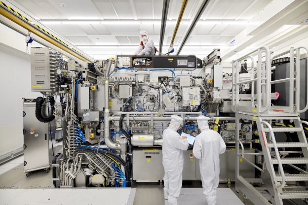
According to Wccftech, TSMC might delay its adoption of High-NA EUV, with the company expected to bypass the tool for its A14 process and instead continue using 0.33-NA EUV, a move revealed by Senior Vice President Kevin Zhang at the NA Technology Symposium and noted by BITS&CHIPS.
Still, the report highlights that TSMC has not ruled out using High-NA EUV, with plans to adopt the technology for its A14P node.
As indicated by the report, TSMC’s decision to skip High-NA EUV may be driven by cost concerns, with the report noting that using the technology could raise production costs by up to 2.5 times compared to conventional EUV methods. This would make manufacturing the A14 node significantly more expensive, potentially limiting its adoption in consumer products.
Notably, the report points out that TSMC’s decision to hold off on High-NA EUV puts it behind competitors like Intel Foundry, which plans to use the technology for its 18A process, which is expected to launch as soon as next year. With TSMC targeting A14P for 2029, the company faces at least a four-year delay in High-NA adoption — a gap that could give rivals an advantage.
Earlier this year in February, Intel revealed that the first two High-NA EUV machines from ASML were already in production, processing 30,000 wafers per quarter, according to Reuters.
Meanwhile, as noted by Korean media outlet The Financial News, citing sources, Samsung Electronics brought in its first High-NA EUV machine, the EXE:5000, to its Hwaseong campus earlier in March.
Read more
(Photo credit: TSMC)


