News

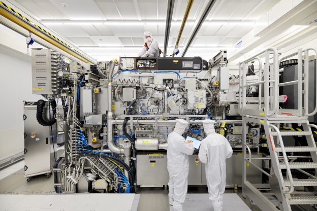
Intel’s early adoption of ASML’s High Numerical Aperture Extreme Ultraviolet Lithography (High-NA EUV) equipment is seen by many as a crucial move for Intel to reclaim its technological leadership. Yet, according to a report from CNA, industry sources cited in the report have warned that the high cost of High-NA EUV could lead Intel to face the dilemma of expanding losses.
As Intel secures High-NA EUV equipment, the Korean media outlet TheElec reported that ASML plans to manufacture five High-NA EUV equipment this year, all of which have been booked by Intel. TSMC’s decision to continue using existing EUV equipment for its A16 process, rather than adopting High-NA EUV, has drawn significant attention and sparked lively discussion.
Per a report from Reuters, Intel CEO Pat Gelsinger has acknowledged that the previous decision to oppose using ASML’s EUV equipment was a mistake, which hampered the profitability of Intel’s foundry business. He stated that, with the adoption of EUV equipment, Intel is now highly competitive in terms of price and performance. There is widespread interest in whether Intel’s early adoption of High-NA EUV equipment will help it regain its position as a technology leader.
On the other hand, TSMC plans to mass-produce its A16 technology by 2026, combining nanosheet transistors with a supertrack architecture, garnering attention from the industry.
Ray Yang, the consulting director at Industry, Science and Technology International Strategy Center of ITRI (Industrial Technology Research Institute), stated that TSMC’s decision not to adopt High-NA EUV equipment for the A16 process was likely made after a comprehensive evaluation.
Yang mentioned that TSMC is undoubtedly aware of the benefits that High-NA EUV equipment can bring. However, given the high costs, TSMC has chosen to meet its customers’ diverse needs through other means.
According to ASML, High-NA EUV equipment increases the numerical aperture from 0.33 to 0.55, providing higher-resolution imaging capabilities. This improvement enhances precision and clarity, simplifies the manufacturing process, reduces production time, and boosts production efficiency.
During a technical symposium in Amsterdam on May 14th, TSMC’s Senior Vice President of Business Development and Co-Chief Operating Officer, Dr. Kevin Zhang, remarked that ‘I like the high-NA EUV’s capability, but I don’t like the sticker price.’
Each EUV system from ASML costs around USD 180 million, while High-NA EUV equipment is priced at USD 380 million, more than double the cost of EUV.
Ray Yang noted that the importance of advanced semiconductor packaging is increasing and will play a crucial supporting role. He argued that Intel’s rush to acquire High-NA EUV equipment is a case of choosing the wrong battlefield and weapon because High-NA EUV equipment is not the sole decisive factor for future success.
Ray Yang stated that as the global leader in semiconductor foundry services, TSMC has numerous customers, a comprehensive ecosystem, and ample capital. If customers demand and are willing to pay higher prices, TSMC will undoubtedly adopt High-NA EUV equipment.
Yang noted that TSMC is taking a cautious approach to adopting High-NA EUV equipment, likely after thoroughly considering its necessity. If Intel makes significant purchases of High-NA EUV equipment, its future capacity utilization will be worth observing, as it might face the risk of increased losses.
Currently, both TSMC and Samsung utilize EUV equipment for manufacturing, covering TSMC’s 7nm, 5nm, and 3nm processes and Samsung’s EUV Line (7nm, 5nm, and 4nm) located in Hwaseong, Korea, along with the 3nm GAA process.
Read more
(Photo credit: ASML)