News

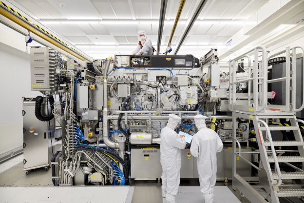
This May, we have witnessed two different approaches to the new High-NA EUV (high-numerical aperture extreme ultraviolet) lithography equipment between semiconductor giants. Intel has secured the first batch of High-NA EUV kits from ASML, which will allegedly be used on its 18A (1.8nm) and 14A (1.4nm) nodes. On the other hand, TSMC stated that the company will not utilize this new lithography technology in its upcoming A16 (1.6nm) process.
High-NA EUV machines may be critical for companies aiming to produce chips beyond 2nm, but are they must-have?
Looking back in history, the industry used to believe that when the U.S. prevented EUV exports to China, the act would limit China’s progress in 7nm. However, China’s largest foundry, SMIC, is rumored to produce 5-nm chips for Huawei this year, without the need for EUV lithography machines.
When examining TSMC’s trajectory on EUV itself, it is worth mentioning that the company took a more cautious stance, as well. When Samsung began using EUV in its 7nm process in 2018, TSMC successfully launched its first 7nm production line using mature DUV lithography.
It was not until the stability and maturity of EUV had been confirmed that TSMC started to use EUV in its N7+ process, which took place in 2019. In the end, in spite of Samsung’s early adoption of EUV, yield issues allowed TSMC to overtake them.
Similarly, in the race for the 3nm process, unlike Samsung, instead of rushing to adopt GAAFET, TSMC chose the reliable FinFET route.
Will history repeat itself? Now it would be a good timing to examine TSMC’s strategy on High-NA EUV machines.
High-NA EUV technology: A Cure for All?
According to a report by China’s Jiwei, at the recent 2024 North America Technology Symposium hosted by TSMC, the company revealed that its A16 process would not require the next-generation High-NA EUV lithography machines, with mass production expected in 2026.
An expert cited by Jiwei stated that TSMC’s decision might be due to the higher risk associated with High-NA lithography machines.
The report noted that there would be still quite a few challenges to be resolved, such as supporting light sources for photon shot noise and productivity requirements, solutions for the 0.55 NA’s small depth of focus, computational lithography capabilities, mask manufacturing, and computing infrastructure including new materials. Not to mention there is the necessary debugging and development time to ensure stability, which implies considerable time and hidden costs.
On the other hand, TSMC began to adopt EUV in its N7+ process in 2019, implying the world’s largest chipmaker has committed plenty of time and effort to refine the technology.
According to the report by Jiwei, by optimizing the EUV exposure dose and the photoresist used, as well as improving photomask life, increasing yield, and reducing defect rates, TSMC has achieved significant advancements. Today, the number of EUV lithography machines has increased tenfold, while wafer output nowadays is 30 times that of 2019.
Weigh Between Cost and Technology
In addition to potential technology bottlenecks, higher cost may be another problem. Per a report from Bloomberg, TSMC’s Senior Vice President of Business Development and Co-Chief Operating Officer, Dr. Kevin Zhang, remarked that while he appreciates the capabilities of High-NA EUV, he finds its price tag to be unlikeable.
As per the same report from Bloomberg, ASML’s new High-NA EUV machine is priced at EUR 350 million (roughly USD 380 million). Jiwei further stated the unit price may more than double, comparing with the current EUV machines (roughly EUR 170 million).
Market demand would be another major concern. Citing an industry insider, Jiwei analyzed that the cost of manufacturing chips with High-NA lithography machines increases significantly. While more chips can be cut from each wafer, more chips need to be sold to recoup the investment.
The report stated that the smartphone AP chip market alone cannot absorb these cost without the supporting demand of AI chips. However, as China, the largest market for AI, is now being restricted by export control measures from the U.S., the overall market demand remain uncertain.
Adoption Timing for High-NA EUV? TSMC May Not Be in a Hurry
Then what would be the right timing for TSMC to adopt High-NA EUV?
The report by Jimwei took the trajectory of EUV as an example. When the industry generally regarded EUV essential in the 7nm node, TSMC successfully launched its first 7nm production line using mature DUV lithography. This strategy allowed TSMC to avoid the imperfections and high costs of EUV lithography at that time.
TSMC waited until 2019 to start the usage of EUV in its N7+ process when the technology has become mature enough. In the end, in spite of Samsung’s early adoption of EUV, yield issues allowed TSMC to win the favor of clients.
Similarly, in the race for the 3nm process, instead of rushing to adopt GAAFET, TSMC chose the reliable FinFET route. Despite Samsung’s early lead with 3nm, their low yields and repeated delays enabled TSMC to surpass them.
TSMC’s previously announced roadmap indicates that the 1.4nm A14 process is expected to be introduced between 2027 and 2028, while the development of the 1nm A10 process is projected to be completed before 2030. The report by Jiwei suggested that TSMC might consider using the next-generation lithography machine only after the 1nm process is in place, potentially adopting the High-NA EUV system around 2029 to 2030.
Read more
(Photo credit: ASML)