News

Amidst the tide of artificial intelligence (AI), new types of DRAM represented by HBM are embracing a new round of development opportunities. Meanwhile, driven by server demand, MRDIMM/MCRDIMM have emerged as new sought-afters in the memory industry, stepping onto the "historical stage." Accordin...
News

South Korean memory giant SK hynix announced on July 26th that it has decided to invest about 9.4 trillion won (approximately USD 6.8 billion) in building the first fab and business facilities of the Yongin Semiconductor Cluster after the board resolution today, according to its press release. Th...
News

As SK hynix and Samsung are releasing their financial results on July 25th and July 31st, respectively, their progress on HBM3 and HBM3e have also been brought into spotlight. Earlier this week, Samsung is said to eventually passed NVIDIA’s qualification tests for its HBM3 chips. While the Big Thr...
News

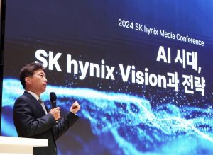
Global HBM leader, South Korea's SK hynix, announced its financial report for the last quarter on July 25, exceeding market expectations. According to a report from Economic Daily News, the company also announced a full-scale effort to boost production of high-bandwidth memory (HBM) for AI, with thi...
News
SK Hynix announced second-quarter revenue of 16.42 trillion Korean won, a 125% year-on-year increase, setting a historical record. ......


