Taiwan


2024-07-01

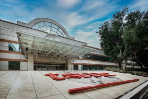
[News] TSMC Achieved a New Step in the Construction of its Third 2nm Fab

Recently, TSMC reportedly got approval for the land change and environmental assessment of its third 2nm plant in Kaohsiung.

It is reported that the Nanzih Industrial Park in Kaohsiung City will adapt to the changing needs of the global semiconductor industry supply chain and will carry out the development of the park in stages. TSMC obtained the construction permit for the first phase of its 2nm advanced process plant in the Nanzih Industrial Park in September 2022, kick starting the construction of first phase, with mass production expected in 2025. The second phase of the plant is also underway.

In response to the shift in the supply chain and the market demand of the global semiconductor industry, TSMC has an urgent need to expand production. The Urban Development Bureau of Kaohsiung City Government stated that TSMC chose to initiate the urban plan variation procedure for the third phase of the plant on the east side of the first phase of the park, covering an area of 17.22 hectares.

To ensure that the industrial use category matches the land use content, the special industrial zone will be changed to a Type A industrial zone, and the building coverage ratio will be adjusted to 45% in consideration of the need of construction, while the original floor area ratio of the special industrial zone will remain at 160%.

Regarding the third 2nm plant, the Kaohsiung City Government’s Water Conservancy Bureau issued a statement saying that the city government fully supports TSMC’s establishment of the plant in the Nanzih Industrial Park, and the reclaimed water supply will be fully guaranteed.

As for electricity, the Economic Development Bureau explained that Kaohsiung’s total power generation in 2022 was 50.886 billion kWh, with total electricity sales of 30.734 billion kWh, accounting for only 60% of power generation. In the future, all TSMC plants will adopt a dual-circuit system to ensure stable power supply.

Previously, Tai-Hsiang Liao, Director of the Economic Development Bureau, pointed out in early April that the city government will provide relevant assistance to meet TSMC’s water and electricity supply needs in Kaohsiung. Additionally, Liao further stated that, based on the current land assessment in the park, the maximum scale of TSMC’s Kaohsiung plant could be up to five plants.

Read more

(Photo credit: TSMC)

Please note that this article cites information from WeChat account DRAMeXchange.

2024-06-26

[News] TSMC Rumored to Build New CoWoS Plant in Southern Taiwan

TSMC’s advanced CoWoS packaging capacity is in severe shortage, and just as the new plant in the Chiayi Park of Southern Taiwan Science Park began construction for expansion, according to a report from Economic Daily News citing sources, it has stated that TSMC intends to build another advanced packaging plant in Pingtung, which is located in southern Taiwan, and is currently in the site selection phase.

Regarding these rumors, TSMC has not yet responded. The relevant authorities, the Taiwanese National Science and Technology Council, stated that they have not heard of this and emphasized that any information about new plant constructions should be released by the company itself.

Currently, TSMC’s in-house packaging and testing capacities are located in Longtan, Hsinchu Science Park, Zhunan, Central Taiwan Science Park, and Southern Taiwan Science Park, with a new plant under construction in the Chiayi Park of Southern Taiwan Science Park. However, construction of one plant in the Chiayi Park was recently suspended due to the possible discovery of a historical site, prompting TSMC to initiate the construction of a second plant in the area.

If the advanced packaging plant in Pingtung is established, TSMC will have seven advanced packaging and testing sites in Taiwan, spanning across Taoyuan, Hsinchu, Miaoli, Taichung, Chiayi, Tainan, and Pingtung.

TSMC Chairman C.C.Wei previously mentioned that the demand for CoWoS capacity exceeds supply. Despite continuous expansion, TSMC still cannot meet all customer needs. Consequently, TSMC has increased outsourcing to professional packaging and testing subcontractors. TSMC is striving to expand its advanced CoWoS packaging capacity, with a target to more than double its in-house capacity this year and continue efforts next year to narrow the gap between supply and demand.

Industry sources cited in Commercial Time’s previous report have further indicated that by the end of next year, TSMC’s monthly CoWoS capacity will be increased to 60,000 wafers. With growing orders and a steep learning curve, the annual capacity is expected to surpass 600,000 wafers next year. As the semiconductor industry advances into the Angstrom Era, the gap in TSMC’s advanced packaging capacity will gradually widen.

Read more

(Photo credit: TSMC)

Please note that this article cites information from Commercial Times and Economic Daily News.

2024-06-25

[News] Leading IC Packaging and Testing Services Provider ASE Expands Globally Amid AI Demand

On June 21, ASE Group announced that ASE Semiconductor will collaborate with Hung Ching Construction to build a K28 plant in Kaohsiung. The project is expected to be completed in the fourth quarter of 2026 and will focus on end testing of advanced packaging processes, and high-performance computing for artificial intelligence (AI) chip.

ASE’s CFO Dong Hongsi introduced that for the K28 plant construction project, ASE Semiconductor will provide the land it held in Kaohsiung while Hung Ching Construction will provide fund support. The plant will have one basement level and seven above-ground floors. As to the rights and value distribution between the two parties, ASE Semiconductor and Hung Ching Construction will respectively hold a share of 22.24% and 77.76%. Upon completion, ASE Semiconductor or its subsidiaries will have the first purchase rights for Hung Ching Construction’s property ownership.

It was reported previously that as an important part of the company’s operational plans, ASE’s Kaohsiung plant had purchased land in Tashe for phased development in a bid to  address the demands for end testing of advanced packaging processes, AI chip high-performance computing, and heat dissipation needs. Phase one, the K27 plant, was completed in 2023, primarily setting up Flip Chip and IC testing production lines.

At a financial result briefing in February this year, ASE stated that to expand advanced packaging capacity, this year’s overall capital expenditure will increase by 40% to 50%, reaching a historical high. Of this, 65% will be allocated to packaging, especially advanced packaging projects, with over 60% used for packaging testing and 30% for electronic manufacturing services.

Moreover, ASE is optimistic about the potential of AI technology and expects AI revenue contributions to double to USD 500 million by the end of 2024 compared to 2023. AI-related revenue is expected to account for a single-digit percentage of the total ATM (Packaging and test) business this year, surpassing last year’s low single digit. And the industry anticipates that next year’s proportion could reach a high single-digit percentage.

Advanced packaging industry has been in high gear in recent years, and ASE has made significant investment in this area over the past two years. In February this year, Infineon and ASE announced that ASE would invest approximately TWD 2.1 billion to acquire Infineon’s two backend assembly and test plants in Philippines and South Korea. This acquisition aims to expand ASE’s  power chip module packaging & test and lead frame packaging for automotive and industrial automation applications, with the transaction expected to be completed by the end of 2Q24.

On January 19, ASE announced that its Malaysian subsidiary would invest MYR 69.696 million to acquire land use right in the Gardenia Tech Park in Penang, Malaysia to meet operational needs. Industry analysts believed this investment was primarily for expanding advanced packaging capacity. It was reported that ASE Semiconductor has been actively expanding its packaging and test capacity in Malaysia. In November 2022, its new factories 4 and 5 in Penang broke ground, with construction expected to be completed by 2025.

Additionally, in late December 2023, ASE Semiconductor announced that it had leased the 7th floors of both K21 and K22 buildings from ASE TEST in Kaohsiung’s Nanzi district to expand its packaging capacity. The industry believed that the intention was to increase its advanced packaging capacity for AI chip.

Read more

(Photo credit: ASE Group)

Please note that this article cites information from WeChat account DRAMeXchange.

2024-06-21

[News] ASE Sets Up New Facility in Kaohsiung for Advanced Packaging, Targeting Completion in 2026 

According to a report from CNA, Taiwanese semiconductor testing and packaging giant ASE announced on June 21st that it will collaborate with Hung Ching Development & Construction Corporation to jointly build the K28 plant in Kaohsiung. Scheduled for completion in Q4 2026, the facility will reportedly focus on advanced packaging and final testing in order to meet the high-performance computing and cooling demands of AI chips.

ASE’s CFO Joseph Tung stated that ASE Semiconductor is planning for operational growth at its Kaohsiung facilities. To meet the demand for advanced packaging processes, high-performance computing for AI chips and cooling, the company is developing land in Dashe, Kaohsiung in two phases. The first phase, K27 plant, was completed and moved-in in 2023, while the K28 plant, the second phase, aims to be completed by Q4 2026.

As reported by CNA citing sources, ASE Kaohsiung Plant contributes approximately 20% to ASE Technology Holding Co., Ltd.’s total revenue. The plant specializes in providing services such as packaging, wafer bumping, probe testing, materials, and final testing. It has also developed several smart factories focusing on advanced processes, including Fan-out packaging, System-in-Package (SiP), wafer bumping, and Flip Chip packaging.

These technologies are primarily used in automotive, medical, IoT, high-speed computing, artificial intelligence, and application processor fields.

Read more

Please note that this article cites information from CNA.

2024-06-17

[News] Venturing into AI, Innolux Reportedly Partners with Memory Giants, While Its 4th Plant in Tainan to Focus on Packaging Applications

Taiwanese panel company Innolux have said to be involving in collaborating with leading global memory manufacturers. According to a report from the Economic Daily News, plans are underway to repurpose its 4th Plant in Tainan (5.5-generation LCD panel plant) for AI-related semiconductor applications, specifically targeting back-end packaging.

Sources cited in the report indicate that, based on the strategies of the top three global memory manufacturers, the partner in this collaboration is likely a memory manufacturer that already has a presence in Taiwan and seeks to expand its capacity there. Innolux’s advantage lies in its advanced panel-level fan-out packaging (FOPLP), which is poised to make a substantial impact in the AI field. However, these reports have not been confirmed by Innolux or any global memory giants.

Regarding the 4th Plant developments at Tainan, Innolux stated on June 16 that, based on flexible strategic planning principles, the company continues to optimize production configurations and enhance overall operational efficiency. Some production lines and products are being adjusted to streamline and strengthen the group’s layout and development.

The surge in AI demand has driven the need for advanced chip heterogenous integration and high-end packaging technologies to meet the high-performance application requirements of AI devices. Targeting these opportunities, Innolux has reportedly repurposed its Tainan 3.5-generation and 4-generation LCD panel production lines for semiconductor-related uses, including FOPLP and X-ray sensors.

Sources cited in the report also revealed that Innolux’s transformation efforts are making progress. After closing the 5.5-generation LCD panel production at the 4th Plant last year, the company has gradually reassigned staff to other facilities. To revitalize capacity and assets, Innolux has been in close contact with leading global memory manufacturers, aiming to develop AI-related applications.

Currently, the three major global memory manufacturers are actively developing high-bandwidth memory (HBM) for AI servers. South Korea’s SK Hynix is the most proactive in collaborating with Taiwanese companies. SK Hynix has partnered with TSMC to aggressively target the AI market. As per a report from Korean media outlet The Korea Herald,  SK Group Chairman Chey Tae-won recently visited TSMC Chairman C.C. Wei to ensure continued close cooperation on the next-generation HBM.

On the other hand, Micron has established memory production in Taiwan but does not yet have HBM capacity for AI servers in the region. Meanwhile, Samsung does not have direct AI cooperation with Taiwanese companies in the memory sector.

Sources cited in the report from Economic Daily News indicate that Innolux is engaging with one of these three major international memory manufacturers, focusing on new semiconductor applications. As Innolux is advancing into the promising glass substrate packaging business through panel-level fan-out packaging, this technology is expected to be combined with memory applications for AI development. Therefore, the developments at its 4th Plant in Tainan are receiving considerable attention.

Read more

(Photo credit: Innolux)

Please note that this article cites information from Economic Daily News and The Korea Herald.

  • Page 6
  • 15 page(s)
  • 71 result(s)

Get in touch with us