Taiwan


2024-05-20

[News] AMD Reportedly Seeks Major Subsidy with Four Conditions from Taiwan Ministry of Economic Affairs

As the era of AI advances, following NVIDIA’s application to the Ministry of Economic Affairs (MOEA) for the “A+ Industrial Innovative R&D Program,”  which led to the establishment of the first R&D center in Asia and the creation of Taiwan’s largest AI supercomputer, “Taipei-1”, American AI chip giant AMD is set to follow suit.

According to a report from UDN, AMD plans to invest NTD 5 billion (roughly USD 155 million) to establish an R&D center in Taiwan and intends to apply for the A+ Industrial Innovative R&D Program from the MOEA, highlighting Taiwan’s critical role in AI chip design and manufacturing.

The MOEA has confirmed that AMD applied for the A+ Industrial Innovative R&D Program subsidy at the end of 2023. However, the funding for the program has already been exhausted. Therefore, funds must be allocated in the fifth phase of the A+ Industrial Innovative R&D Program, with the science and technology budget to be set for 2025.

This budget allocation must be approved by the new government administration. Additionally, MOEA officials stated that AMD must submit a concrete plan and gain approval from a review committee established by the Industrial Technology Department of the MOEA.

Previously, the MOEA’s substantial subsidies to global companies under the A+ Industrial Innovative R&D Program sparked mixed reactions within the industry. Some prominent local IC design companies criticized the MOEA, arguing that supporting global companies leads to competition against local businesses and drains valuable local R&D talent.

To avoid controversy, the MOEA has set forth four specific requirements for AMD.

First, they hope AMD will collaborate with Taiwanese IC design companies. Second, any AI servers developed should be manufactured in Taiwan. Third, at least 20% of the R&D workforce should be sourced from abroad, and high-level executives should be stationed in Taiwan. Fourth, AMD should partner with Taiwanese universities to cultivate talent jointly. The MOEA reports that AMD’s response has been very positive, and a thorough review of the application will take place in the second half of the year.

To date, the MOEA’s A+ Industrial Innovative R&D Program has approved subsidies only for two global companies, Micron and NVIDIA, providing them with NTD 4.722 billion (USD 146.48 million) and NTD 6.7 billion (USD 207.8 million), respectively. The MOEA believes this strategy helps solidify Taiwan’s competitive edge in the global semiconductor and AI sectors.

Read more

(Photo credit: AMD)

Please note that this article cites information from UDN.

2024-04-29

[News] Overseas Expansion of Testing and Packaging Facilities – Japan, Malaysia, and Singapore Emerge as Top Choices

As the global semiconductor landscape undergoes restructuring, major packaging and testing companies are actively establishing overseas advanced packaging capacities. According to a report from Commercial Times, semiconductor industry sources have indicated that, in terms of the clustering effect within the semiconductor industry, the primary targets currently include Japan, Malaysia, and Singapore.

Industry sources cited by the same report have pointed out that the global top ten packaging and testing companies are dominated by Taiwan, China, and the United States. Taiwan holds the lead with five industry giants including ASE Group, Powertech Technology, King Yuan Electronics CO. (KYEC), Chipbond Technology, ChipMos and Sigurd.

China boasts four key players such as Jiangsu Changjiang Electronics Technology Co., Tongfu Microelectronics, and Huatian Technology Co. Meanwhile, the United States is represented by Amkor, the world’s second-largest in scale. Japan’s pursuit of rebuilding the packaging and testing industry through a foundry model and seeking support from Taiwanese companies can be seen as a logical progression.

Given that nine out of the top ten packaging and testing companies are located in the Asia-Pacific region, the strategic positioning in Asia is particularly notable, with Japan, Malaysia, and Singapore all striving to make their mark.

Industry sources cited by the same report point out that Malaysia has been developing its semiconductor industry for decades, with Penang being a prominent semiconductor hub. Not only does Penang boast technological advantages, but it is also dubbed the “Silicon Valley of the East.”

As companies like TSMC, Samsung, and Intel expand their fabs to locations such as the United States and Europe, the downstream semiconductor testing and packaging activities are gradually forming clusters in Malaysia. This includes ASE Group’s significant investment in building a new testing and packaging facility in Penang, scheduled for completion in 2025.

Intel is also planning to establish advanced packaging facilities in both Penang and Kedah. Additionally, Texas Instruments from the United States has announced plans to build semiconductor testing and packaging facilities in Kuala Lumpur and Malacca.

While Malaysia’s testing and packaging sector has become a hub, industry sources cited by the report point out that despite many countries aggressively building their semiconductor industry chains, Japan is seen as the country, outside of Taiwan, with the most comprehensive semiconductor supply chain in the future, due to factors such as cultural traits, industrial development experience, geographical proximity to Taiwan, and long-standing close cooperation.

TrendForce has previously reported that Japan’s resurgence in the semiconductor arena is palpable, with the Ministry of Economy, Trade, and Industry fostering multi-faceted collaborations with the private sector. With a favorable exchange rate policy aiding factory construction and investments, the future looks bright for exports.

With Japan rapidly catching up in development, it becomes necessary for companies like ASE Group to strengthen their presence in Japan. The sources cited by the report are optimistic that Taiwanese-owned testing and packaging facilities may follow suit.

Recently, Powertech Technology Inc., Taiwan’s testing and packaging company, expressed openness to exploring opportunities in Japan, including seeking subsidies from the Japanese government, following the model set by TSMC.

Singapore is also actively strengthening its semiconductor industry chain. Per official Singaporean data, out of the 15 world-class chip design companies, 9 have established bases in Singapore. Additionally, there are 14 semiconductor fabs and 20 semiconductor assembly and testing facilities.

Coupled with the nearby established backend testing clusters in Malaysia, if Singapore constructs a more complete industry chain, it is poised to attract even more world-class testing and packaging companies to establish their presence there.

Read more

Please note that this article cites information from Commercial Times.

2024-04-19

[News] TSMC to Recognize NTD 3 Billion Earthquake Loss

Following the magnitude 7.2 earthquake in Taiwan on April 3rd, all of TSMC’s fabs resumed normal operations within three days. According to a report from Commercial Times, TSMC expects to recognize earthquake-related losses of approximately NTD 3 billion (roughly USD 92.1 million) in the second quarter after deducting insurance claims.

During its earnings call on April 18th, TSMC President C.C. Wei expressed gratitude for the dedication and hard work of all employees and supplier partners. He also thanked customers for their understanding and support, stating that TSMC would compensate for production losses in the second quarter.

C.C. Wei stated that during this earthquake, the maximum intensity experienced at TSMC’s fabs was level 5. Immediately following the earthquake, TSMC activated safety measures and occupational health systems at the fabs. All personnel were safe, and through everyone’s tireless efforts, plant operations were swiftly restored.

Due to TSMC’s extensive experience and capabilities in earthquake response and disaster prevention, coupled with regular safety drills, the overall equipment recovery rate of TSMC’s fabs exceeded 70% within 10 hours of the earthquake and was fully restored before the end of the third day following the earthquake. There were no power outages or structural damages at TSMC’s fabs, including critical equipment such as extreme ultraviolet (EUV) exposure machines, all of which remained undamaged.

During this earthquake, although TSMC experienced a certain quantity of wafers in production that were affected and had to be scrapped, it is anticipated that most of the production losses will be recovered in the second quarter, resulting in minimal impact on second-quarter revenues.

TSMC expects the overall impact of the earthquake to decrease its second-quarter gross margin by approximately 50 basis points, primarily due to losses related to wafer scrap and material consumption.

Read more

(Photo credit: TSMC)

Please note that this article cites information from Commercial Times.

2024-04-16

[News] PSMC’s Q1 Loss Narrows, while Q2 Shipments Impacted by Earthquake, Down 5%-8%

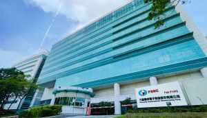
The Taiwanese semiconductor foundry Powerchip Semiconductor Manufacturing Corporation (PSMC) has held its earnings call and released its Q1 financial report. According to a report from Liberty Times Net citing information, with increasing capacity utilization, idle capacity costs decreased, boosting gross margin to 15.4%, up 12.3 percentage points from the previous year’s Q4. The net loss narrowed to NTD 439 million after tax, translating to a loss of NTD 0.11 per share.

Looking ahead to a potential turnaround this year, PSMC’s General Manager, Brian Shieh, highlighted that while large-size panel driver ICs are performing relatively well, Chinese foundries are exerting significant pricing pressure on mature processes, impacting average selling prices unfavorably. This remains a key variable affecting profitability.

In response to inflation-driven equipment cost adjustments and market demands, PSMC is revising its product portfolio. They also announced an increased capital expenditure of NTD 32 billion for 2024, which represents a 30% increase from the previously disclosed amount of NTD 24 billion. Powerchip’s Tainan fab has initiated trial production, with future investments focusing on power management IC, memory, and copper processes in the interposer.

Brian Shieh mentioned that PSMC’s capacity utilization rate was around 65% in the fourth quarter of last year. In the first quarter of this year, the utilization rate for logic products improved slightly, while memory product utilization reached 95% to 98%.

He expects memory product utilization to remain at first-quarter levels in the second quarter, with logic product utilization around 65% to 70%. Overall gross margin is anticipated to remain stable or improve compared to the first quarter.

According to TrendForce’s previous report on the fourth quarter of 2023, global semiconductor foundry revenue rankings showed that Intel Foundry Services (IFS), which ranked ninth globally in the third quarter of 2023, was pushed out of the top ten by PSMC and Nexchip due to factors such as the transition between old and new CPU generations and lackluster inventory momentum. At the same time, the top three semiconductor foundries globally were TSMC, Samsung, and GlobalFoundries.

Read more

(Photo credit: PSMC)

Please note that this article cites information from Liberty Times Net.

2024-04-15

[News] TSMC Reportedly Accelerates 2nm Progress, with Kaohsiung Plant Rumored to Commence First Tool-in by Year-end

TSMC, the leading semiconductor foundry, recently announced plans to establish a 2nm production line in the US, while attention remains on expansion progress in Taiwan.

According to a report from MoneyDJ, it has indicated that the 2nm fab in Hsinchu’s Baoshan is proceeding steadily as planned, and the 2nm fab in Kaohsiung is gaining momentum, with the first tool-in expected by year-end.

Initially, both fabs will achieve a monthly capacity of approximately 30,000 to 35,000 wafers. By 2027, their combined capacity is set to exceed 100,000 wafers, marking the mainstream transition to the next generation of processes.

As per industry sources cited by MoneyDJ, TSMC’s 2nm production bases are located in Hsinchu Science Park and Kaohsiung, and Baoshan’s Phase 2 will begin tool-in in the second quarter, with a “mini line” to be established by year-end and mass production targeted for Q4 2025, starting with an initial monthly capacity of approximately 30,000 to 35,000 wafers.

Meanwhile, the Kaohsiung plant is expected to commence equipment installation by year-end, ahead of the original schedule, aiming for mass production in the first half of 2026 with an initial monthly capacity plan similar to Baoshan’s 30,000 to 35,000 wafers.

The same sources also indicate that after the formal mass production of the Baoshan and Kaohsiung plants, they will enter the capacity ramp-up phase, aiming to achieve a combined capacity of around 110,000 to 120,000 wafers per month by 2027. Both fabs will produce the first-generation 2nm and the second-generation N2P with backside power rail technology. The next-generation 1.4nm (A14) is expected to commence production in the second half of 2027, potentially located in Taichung.

In the 2nm client landscape, Apple remains a frontrunner, earmarking the technology for flagship smartphones. Intel has also expressed interest, with AMD, NVIDIA, and MediaTek expected to follow suit.

Looking at the process roadmap, this year’s iPhone 16 will use N3E, while next year’s model will adopt N3P. Thus, the first consumer product leveraging TSMC’s 2nm process is anticipated to launch in 2026.

Previously at its earnings call, TSMC disclosed the development of a backside power rail solution for N2, tailored for HPC applications.

TSMC is scheduled to hold an earnings call on April 18th. It is anticipated that the related topics around its 2nm process will also be the focus of attention on the day of the conference.

Read more

(Photo credit: TSMC)

Please note that this article cites information from MoneyDJ.

  • Page 9
  • 15 page(s)
  • 71 result(s)

Get in touch with us