Popular Keywords


UMC
News
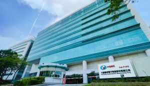
[News] PSMC’s Japanese Venture in Mie Prefecture Awaits Local Support
According to UDN News, Taiwan's semiconductor foundry, Powerchip Semiconductor Manufacturing Corporation (PSMC), is planning to establish a 12-inch wafer plant in Japan, with Mie Prefecture emerging as a probable location. This facility will be part of a burgeoning semiconductor hub that links up wi...
News

[News] UMC and ASE Weigh Price Increases in Booming Advanced Packaging Market
According to a report by Taiwan's Economic Daily, TSMC is aggressively expanding its advanced packaging capacity. Recently, they placed an additional 30% order for equipment with manufacturers, leading to a doubling of order volumes for companies in the interposer supply chain, such as UMC and ASE G...
News

[News] 8-Inch Wafer Fabs to Increase Monthly Production Capacity by 14% in 2026
Source to China Times, the International Semiconductor Industry Association (SEMI) forecasts that from 2023 to 2026, the global semiconductor industry will add 12 new 8-inch wafer fabs, with 8-inch fab monthly production capacity increasing by 14% to a historic high of 7.7 million wafers. In respons...
News

[News] Goldman Sachs Securities Downgrades TSMC’s Next Year Capex
According to a report by Taiwan's Media TechNews, Taiwan's leading semiconductor foundry, TSMC (Taiwan Semiconductor Manufacturing Company), experienced a significant 2.43% decline in its ADR (American Depositary Receipt) on the last trading day of the previous week in the U.S. stock market. This dr...
News

[News] Recovery in Foundry Mature Node May Be Delayed Until Next Year
According to the news from ChinaTimes, the semiconductor market is experiencing a slowdown, with Taiwan's three major mature process wafer foundries UMC, VIS, and PSMC all reporting reduced revenues in August. VIS and UMC both posted lower revenues compared to the previous month, while PSMC managed ...
- Page 9
- 15 page(s)
- 75 result(s)